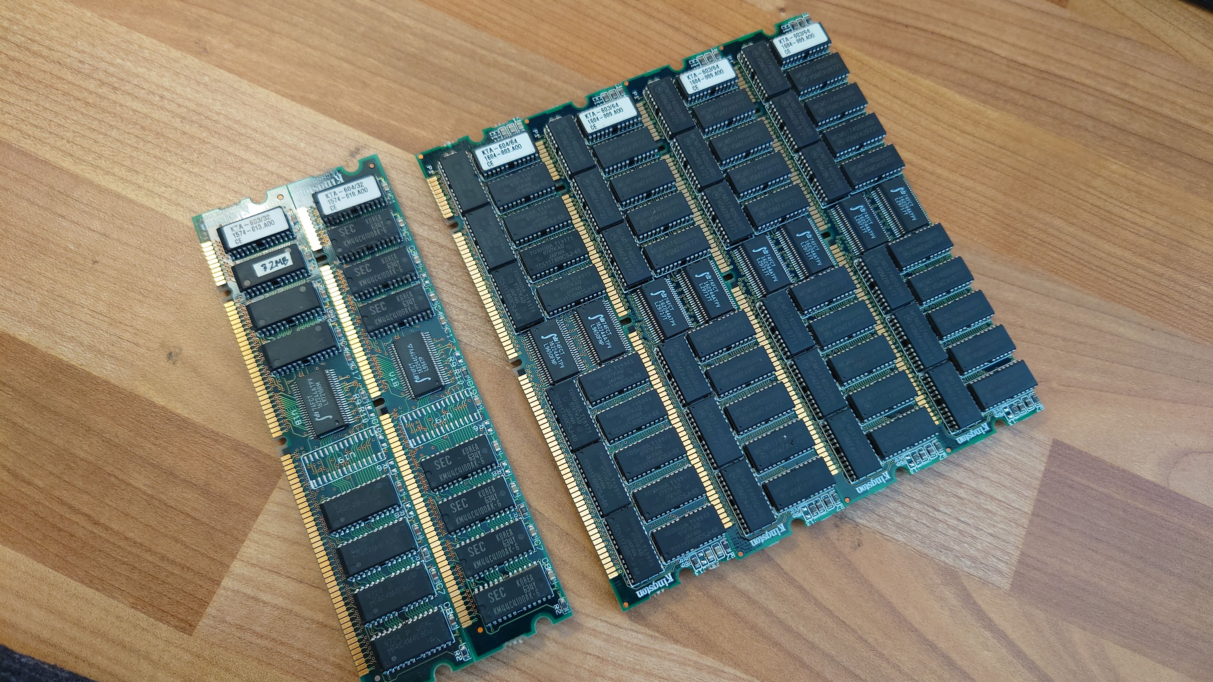
Or the memory maker could have just been crossing their fingers that the memory chips wouldn't blow out before they closed up shop and disappeared.
Yes it’s a bit of this but also there are legit 5V tolerant 3.3V DRAMs. The difference between a 5V tolerant 3.3V DRAM and one that's not is in the input protection circuit. The "classic CMOS" protection circuit is employed on a chip is a set of diodes sort of from ground to the pin and from the pin to Vcc. Thus input signals beyond the supply rails are clamped. Here's a picture:
Of course, if Vcc is 3V and you apply a 5V signal to the pin, the 5V signal sort of gets shorted to the 3V Vcc through the ESD diode. This in and of itself is not necessarily bad. If you check the datasheet for 74HC-series logic, you see that they support +/- 25 mA of clamp current. So with this setup you can do input level translation by putting the right size of resistor in series with the pin to limit the clamp current to acceptable levels. Check this picture from the Altera MAX II datasheet:
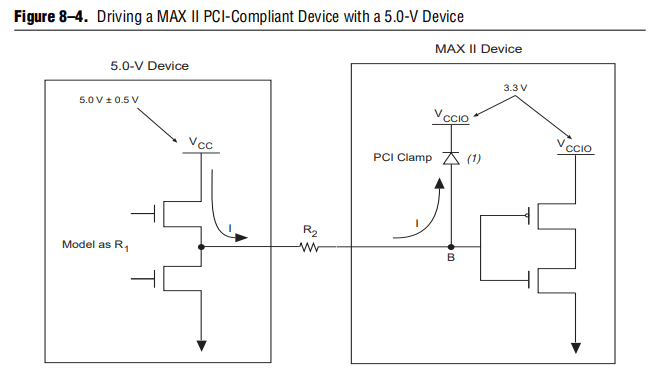
Now, there are some problems with this approach. Firstly, I don't think you're supposed to do it with DRAMs. You've gotta keep to the clamp current spec in the datasheet and if it's not listed then don't try this approach. To keep the clamp current reasonable, the resistor has to be in the range of 100-1000 ohms. If you have a 10 pF input, 1000 ohms adds an extra ~10ns propagation delay going in. Going out is even worse. Imagine you're trying to drive a 100 pF bus (not even that much). 1000 ohms adds 100ns delay. So this approach is only good for slowish inputs, not bidirectional signals like a RAM data bus.
So some chips have a different ESD diode approach. The key issue with the previous approach is the clamp current. To address this, some ICs stack several protection diodes going to Vcc. Therefore the pin only clamps when the input is multiple diode drops above Vcc and thus a chip powered at 3.3V can have 5V signals applied without clamping. Or the upper clamp is removed and the lower clamp diode is replaced with something along the lines of a zener, with a controlled reverse breakdown voltage above 5V.
This is the approach used by the few 5V-tolerant 3V DRAMs. Advantage is that you can just directly connect them to a 5V bus. Since most 5V chips work with TTL-level inputs where < 0.8V is a 0 and > 2.0V is a 1, the 5V TTL thresholds basically line up perfectly with a 3V CMOS chip whose outputs go nearly to the rails when unloaded. So no problem with the 5V chips understanding the 3V logic.
The problem is, as usual, a parts supply thing. We can make the board, put the 3V regulator on, etc., but it may be difficult to source chips that are actually 5V tolerant and we can be sure of it. Lemme illustrate my point.
This is from the datasheet for the KM48V8100B, an 8Mx8 FPM DRAM. Notice in recommended operating conditions, max input voltage is 5.5V or 6.5V for short pulse widths:
Now from the KM48V8100C datasheet... same chip, just revision C, right? Nope, max input voltage is Vcc+0.3 (indicating the presence of the upper clamp diode):
So it's hard to get the right chips. Remanufactured ICs are a no-no, because who can say whether they're actually the revision claimed? Everyone just sort of ignores the revision letter at the end of the part number because they're seen as basically interchangeable.
Now I had an interesting experience that led me to discover all this. I bought like 10 72-pin SIMMs on eBay. All had remanufactured Micron chips. The datasheet for the part numbers on the chips suggested they weren't 5V tolerant and had the clamp diodes. But then I did an input clamp current test and could detect absolutely no difference in input current as the pin went above 3.3V. For a 5V CMOS DRAM, taking the pin more than 1V above Vcc would certainly cause a bunch of input current through the ESD diode. So were the chips mislabeled and actually 5V tolerant? Was Micron being conservative, or did they attempt to engineer 5V tolerance into their chips but were not successful enough to spec it? Who knows...